Flip chip bonder (for Chip on Substrate)
Capable of stacking application in various programs for handling 3D packaging.
Can be used for various work processes and devices, such as flux, NCP, NCF, Cu pillars, and TSV.
Ultra-low pressure head; dispenser; flux; bonding inspection unit; upper communication, etc.
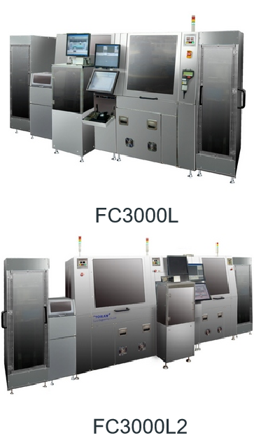
FC3000L
Line configuration: loader, dispenser unit, chip loader, packaging unit, unloader
FC3000L2
Line machine with two bonders.
Line configuration: loader, dispenser unit, packaging unit, chip loader, packaging unit, unloader
|
Specification/Model |
FC3000L |
FC3000L2 |
|
|
Machine type |
Line configuration: loader, dispenser unit, packaging unit, chip loader, and unloader. |
Line configuration: loader, dispenser unit, packaging unit, chip loader, packaging unit, and unloader. |
|
|
Substrate size (mm) |
125–250 mm long x 40–95 mm wide (t=0.2–1.0 mm) |
125–250 mm long x 40–95 mm wide (t=0.2–1.0 mm) |
|
|
Chip size(mm) |
Thermo-compression bonding *1 |
3.0–20 mm long x 3.0–20 mm wide (t=0.05–1.0 mm) |
3.0–20 mm long x 3.0–20 mm wide (t=0.05–1.0 mm) |
|
Ultra-low pressure bonding |
3.0–20 mm long x 3.0–20 mm wide (t=0.05–1.0 mm) |
3.0–20 mm long x 3.0–20 mm wide (t=0.05–1.0 mm) |
|
|
Chip type |
Wafer:1 |
Wafer:1 |
|
|
Chip orientation *2 |
Face up (Wafer 8",12") |
Face up (Wafer 8",12") |
|
|
Cycle time *3 |
1.8sec/chip |
1.8sec/chip |
|
|
Alignment accuracy (3 σ) *4 |
±2μm(X,Y) |
±2μm(X,Y) |
|
|
Pressurization force(N) |
High-stiffness head |
9.8-490 |
9.8-490 |
|
Ultra-low pressure head |
0.098–9.8 |
0.098–9.8 |
|
|
Bonding head type |
Ceramic heater head: temperature RT–450℃ |
Ceramic heater head: temperature RT–450℃ |
|
Notes:
*1 Large-sized chip (max. 30.0 mm long x 30.0 mm wide) can be processed as an option.
*2 8" wafer and waffle tray can be processed with options.
*3 Cycle time does not include processing time (i.e. searching, bonding and vacuum release).
*4 Accuracy measurement is taken using Toray-standard substrates.

東麗工程株式會社(Toray Engineering Corporation)是總部位於日本的綜合性工程及自動化生產設備製造公司,其業務包括生產和銷售用於平板顯示器及半導體生產的自動化生產檢測設備及各種製造業使用的檢測與監控儀器等。Toray 旗下INSPECTRA系列AOI在提供超高精度的晶圓表面缺陷全自動檢測的同時, 具有速度快,穩定度高的特點。此外,TORAY INSPECTRA AOI對Bumping, Sawn Wafer 等製程提供有效並獨特的檢測方案。Toray 還提供業內高精度的TCB/FC設備,用於chip to wafer/ substrate的 高精度die bonding solution。 同時,Toray可以提供客戶不同應用的設備,FC/TCB bonder有不同精度速率和設備來達到客戶不同的需求。
聯絡請洽:http://www.spirox.com.tw/contact