Capable of stacking application in various programs for handling 3D packaging.
Can be used for various work processes and devices, such as flux, NCP, NCF, Cu pillars, and TSV.
|
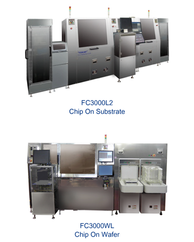
FC3000L2 (for Chip on Substrate)
|
|||
|---|---|---|---|
|
Machine Type
|
Line configuration: loader, dispenser unit, packaging unit, chip loader, packaging unit, and unloader.
Fully automatic machine with increased production capability using two packaging units.
|
||
|
Substrate Size (mm)
|
125–250 mm long x 40–95 mm wide
(t=0.2–1.0 mm)
|
||
|
Chip size(mm)
|
Thermo-compression Bonding *1
|
3.0–20 mm long x 3.0–20 mm wide
(t=0.05–1.0 mm)
|
|
|
Ultra-low Pressure Bonding
|
3.0–20 mm long x 3.0–20 mm wide
(t=0.05–1.0 mm)
|
||
|
Chip Type
|
Wafer:1
|
||
|
Chip Orientation *2
|
Face up (Wafer 8",12")
|
||
|
Cycle Time *3
|
1.8 sec/chip
|
||
|
Alignment Accuracy (3 σ) *4
|
±2μm (X,Y)
|
||
|
Pressurization Force(N)
|
High-stiffness Head
|
9.8 – 490
|
|
|
Ultra-low pressure Head
|
0.098 – 9.8
|
||
|
Bonding Head Type
|
Ceramic heater head: temperature RT–450℃
|
||
|
FC3000WL (for Chip on Wafer)
|
||
|---|---|---|
|
Machine Type
|
COW bonder with chip loader and wafer loader/unloader for mass production use
|
|
|
Substrate Size (mm)
|
8”, 12” t=0.725-1(㎜)
|
|
|
Chip Size(mm)
|
Thermo-compression Bonding *1
|
3–20 mm long x 3–20 mm wide
(t=0.05–1.0 mm)
|
|
Chip Type
|
1
|
|
|
Chip Loading Method
|
Wafer or tray pallet
|
|
|
Chip Orientation
|
Face up
|
|
|
Cycle Time *2
|
2.0 sec/chip
|
|
|
Alignment Accuracy (3 σ) *4
|
±2μm (X,Y)
|
|
|
Bonding Head Type
|
Ceramic heater head:temperature RT-450℃
|
|

Toray Engineering Corporation is a comprehensive engineering and automatic production equipment manufacturing company headquartered in Japan. Its business includes the production and sales of automatic production testing equipment for flat panel display and semiconductor production, as well as testing and monitoring instruments used in various manufacturing industries. The INSPECTRA series AOI of Toray is characterized by high speed and high stability while providing ultra high precision automatic detection of wafer surface defects. In addition, TORAY INSPECTRA AOI provides an effective and unique detection scheme for Bumping, Sawn Wafer and other processes. Toray also provides high-precision TCB/FC equipment in the industry for the high-precision die bonding solution of chip to wave/abstract. At the same time, Toray can provide customers with equipment for different applications. FC/TCB bonders have different precision rates and equipment to meet different customer needs.