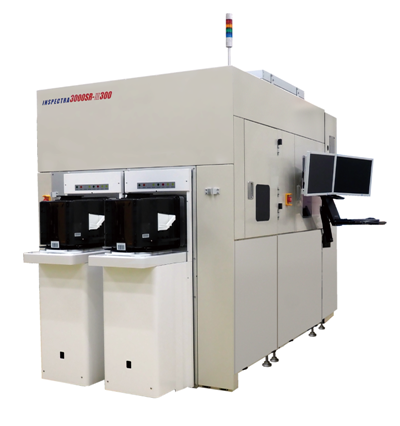
✔ INSPECTRA® Series meet the requests of 100% automatic inspection with high speed and high specifications from front-end to back-end of semiconductor processing.
✔ The original "Die-to-Statistical-Image" comparison method achieves the target defects detection controlling process variation and overkill.
|
|
Feature |
Advantage
|
|---|---|---|
|
Large FOV with Small Pixel Size
|
High speed and high sensitivity
|
High throughput with good detection result
|
|
Die-to-Statistical-Image Algorithm
|
Achieve the target defects detection
|
Control process variation and overkill
|
|
Various Lineup Optical and Hardware Systems
|
Provide optimal detection solutions
|
Applicable for various wafer size and types
|
|
INSPECTRA® Series
|
|
|---|---|
|
Applicable Wafer Size Type
|
2~12 inch, Silicone wafer / Framed wafer / Compound wafer / Glass etc.
|
|
Target Defect Size
|
> 0.5 μm
|
|
Application
|
Front side / Backside / Edge
|
|
Usage Track Record
|
LSI, CISs, MEMS, LED, Bump/TSV/Via Inspection, Power Semiconductor, SiC, GaN, Compound Semiconductor
|

The corporate philosophy of the Toray Group is contributing to society through the creation of new values.
TASMIT, a member of Toray Engineering Group, executes this corporate philosophy with the aim of becoming a company that is highly valued by all of its stakeholders including customers, shareholders and employees.
To do this, TASMIT will contribute to solving social issues through its business and implement the idea of Creating Shared Value (CSV), which combines social values with corporate values.
TASMIT promises to provide effective solutions for the semiconductor device manufacturing with our two core technologies: optical wafer inspection "Inspectra" and electron wafer pattern inspection "NGR".