The inverted emission microscope is a backside analysis system designed to identify failure locations by detecting the light and heat emitted from the defects in semiconductor devices.
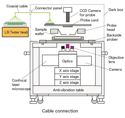
The signal detection from backside facilitates the use of probing and probe card to the wafer surface, and the sample setting can be performed smoothly. The platform, possible to mount multiple detectors and lasers, enables the selection of the optimum detector for performing various analysis methods such as light emission and heat generation analysis, IR-OBIRCH analysis, and others; moreover, letting dynamic analysis perform efficiently by tester connection.
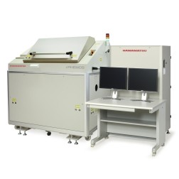
●iPHEMOS-MP
Support for measurement from a single chip to a wafer by mounting a 300 mm wafer prober. Multi-pin needle contact by probe card and sample observation on PC board are available. Dynamic analysis with LSI tester drive is also possible by cable connection.
The iPHEMOS-MP superimposes the emission image on a high-resolution pattern image to localize defect points quickly. The contrast enhancement function makes an image clearer and more detailed.
Display function
| Line voltage | AC 200 V (50 Hz/60 Hz) |
|---|---|
| Power consumption | Approx. 1400 VA (Max. 3300 VA) |
| Vacuum | Approx. 80 kPa or more |
| Compressed air | 0.5 MPa to 0.7 MPa |
| Dimensions/Weights | Main unit: 1740 mm (W)×1150 mm (D)×1770 mm (H), Approx. 1400 kg Control rack: 880 mm (W)×700 mm (D)×1542 mm (H), Approx. 255 kg Optional desk: 1000 mm (W)×800 mm (D)×700 mm (H), Approx. 60 kg |
*Weight of iPHEMOS-MP main unit includes a prober or equivalent item.

Founded in 1953, HAMAMATSU Photonics Co., Ltd., is the pioneer of science and technology, coupled with the massive market share of optics science and EFA market. Hamamatsu Group's products are widely used in medical biology, high-energy physics, space exploration, precision analysis and other industries, is the optical industry leader. HAMAMATSU, with largest customer base in semiconductor and display industry, provides leading EFA solutions, OBIRCH emission microscope with high resolution location detection devices, and other professional optical products with technology patents. HAMAMATSU products are equipped with thermal, EMMI, OBIRCH functions.
Contact and consultation:http://www.spirox.com.tw/contact/contact-product